Scanning tunneling microscopy (STM) of high Tc cuprates
What is a Scanning Tunneling Microscope?
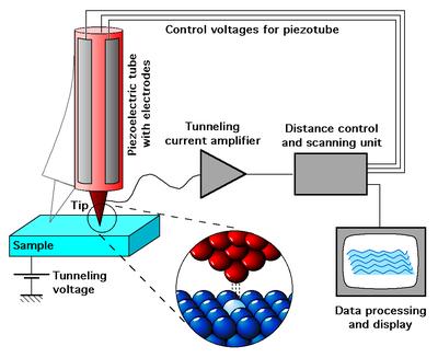
A scanning tunneling microscope (STM) is an incredibly useful device that uses the concept of quantum tunnelling to investigate surfaces using electrons. STM are able to produce a three dimensional profile of the surface of a metal on the atomic level. The STM, which was invented in the early 1980s by Gerd Binnig and Heinrich Rohrer, was of such importance that it was worthy of the Nobel Prize in Physics. For the STM to work, the sharp tip must be moved just slightly above the area of interest. At this point, electrons tunnel quantum mechanically across the gap from the tip to the area, investigating the density of states (DOS) of the object.
Instrumentation
The most important elements of the STM would have to be the scanning tip and the transducers. Tungsten is generally used when constructing the tip, although Platinum-Iridium and Gold are also used. It is crucial that the tip of the STM be extremely sharp (ending in a single atom)to provide the most accurate imaging when used. The piezoelectric transducers play an important role as they allow for independent motion in the x, y, and z planes. Also, spring systems are often used in STM in order to minimize the vibrations caused by the tunnel current. Without these spring systems, it would be very difficult to interpret the data.
Tunneling
As was previously stated, the basic principles of the STM are those of quantum mechanics; specifically tunneling. The idea behind tunneling is that objects of very small mass have a quantifiable probability of passing through other objects due to the wavelike nature in which it moves.
In a one-dimensional case, with the presence of a potential U(z), one can find that the electrons energy levels ψn(z) are found by solutions to Schrödinger's Equation,
- ,
ħ = reduced Planck’s constant, z = position, and m = mass of an electron.
In the area between the STM and the material,E < U(z) so the wave functions which satisfy this are decaying waves,
- ,
with
measuring the decay of the wave inside the barrier.
The probability density for an electron to be found at some location can be determined through the wave function. Let us assume the barrier width is W. This probability, P, that an electron at z=0 (left edge of barrier) can be found at z=W (right edge of barrier) is proportional to the wave function squared,
- .
If the bias is small, we can let U − E ≈ φM in the expression for κ, where φM, the work function, gives the minimum energy needed to bring an electron from an occupied level, the highest of which is at the Fermi level (for metals at T=0 kelvins), to vacuum level. When a small bias V is applied to the system, only electronic states very near the Fermi level, within eV, are excited. These excited electrons can tunnel across the barrier. In other words, tunneling occurs mainly with electrons of energies near the Fermi level.
However, tunneling does require that there is an empty level of the same energy as the electron for the electron to tunnel into on the other side of the barrier. It is because of this restriction that the tunneling current can be related to the density of available or filled states in the sample. The current due to an applied voltage V (assume tunneling occurs sample to tip) depends on two factors: 1) the number of electrons between Ef and eV in the sample, and 2) the number among them which have corresponding free states to tunnel into on the other side of the barrier at the tip. The higher density of available states the greater the tunneling current. When V is positive, electrons in the tip tunnel into empty states in the sample; for a negative bias, electrons tunnel out of occupied states in the sample into the tip.
Mathematically, this tunneling current is given by
- .
One can sum the probability over energies between Ef − eV and eV to get the number of states available in this energy range per unit volume, thereby finding the local density of states (LDOS) near the Fermi level. The LDOS near some energy E in an interval ε is given by
- ,
and the tunnel current at a small bias V is proportional to the LDOS near the Fermi level, which gives important information about the sample. It is desirable to use LDOS to express the current because this value does not change as the volume changes, while probability density does. Thus the tunneling current is given by
where ρs(0,Ef) is the LDOS near the Fermi level of the sample at the sample surface. By using equation (6), this current can also be expressed in terms of the LDOS near the Fermi level of the sample at the tip surface,
The exponential term in (9) is very significant in that small variations in W greatly influence the tunnel current. If the separation is decreased by 1 Ǻ, the current increases by an order of magnitude, and vice versa. A. Bonnell and B. D. Huey “Basic principles of scanning probe microscopy” from Scanning probe microscopy and spectroscopy: Theory, techniques, and applications 2nd edition Ed. By D. A. Bonnell Wiley-VCH, Inc. New York (2001)</ref>.
This approach fails to account for the rate at which electrons can pass the barrier. This rate should affect the tunnel current, so it can be accounted for by using Fermi’s Golden Rule with the appropriate tunneling matrix element. John Bardeen solved this problem in his study of the metal-insulator-metal junction, MIM[1]. He found that if he solved Schrödinger’s equation for each side of the junction separately to obtain the wave functions ψ and χ for each electrode, he could obtain the tunnel matrix, M, from the overlap of these two wave functions. This can be applied to STM by making the electrodes the tip and sample, assigning ψ and χ as sample and tip wave functions, respectively, and evaluating M at some surface S between the metal electrodes at z=zo, where z=0 at the sample surface and z=W at the tip surface.
Now, Fermi’s Golden Rule gives the rate for electron transfer across the barrier, and is written
- ,
where δ(Eψ-Eχ) restricts tunneling to occur only between electron levels with the same energy. The tunnel matrix element, given by
- ,
is a description of the lower energy associated with the interaction of wave functions at the overlap, also called the resonance energy.
Summing over all the states gives the tunneling current as
- ,
where f is the Fermi function, ρs and ρT are the density of states in the sample and tip, respectively. The Fermi distribution function describes the filling of electron levels at a given temperature T.
Superconductors
Superconductivity is a quantum mechanical principle, which is characterized by materials having zero resistance (electrical) as well as not having an interior magnetic field. This will usually occur when a given material is at very low temperatures, although there are specific materials which do not follow this trend.
In conductors, defects and impurities in the material will cause the critical temperature to be lower. However, for a superconductor, the electrical resistivity drops to zero when the material is cooled below the limit, despite whichever imperfections it may have. Now, it is true that superconductivity may occur in many different materials. These materials range from heavily-doped semiconductors, to elements such as aluminum and tin. Even some metallic alloys are able to become superconductive. However, metals such as gold and silver, as well as other noble metals, are not able to become superconductive.
Renewed interest in superconductivity was sparked in 1986, when high temperature superconductors were discovered. Unlike traditional superconductors at the time, with Tc in the range of 20 K, these high temperature superconductors possessed Tc that were around 90 K. This discovery came in the form of cuprate-perovskite ceramic materials. As great as this achievement was (finding material with Tc=90K), it was just the first move into research that is still going strong today.
High Tc Cuprates
Many of the concepts that are too be discussed in this section will be covered in greater detail in the following sections of this report. Some of the more important concepts to consider are the Mott insulators,
Cuprate superconductors are generally considered to be quasi-two-dimensional materials with their superconducting properties determined by electrons moving within weakly coupled copper-oxide (CuO2) layers. Neighbouring layers containing ions such as La, Ba, Sr, or other atoms act to stabilize the structure and dope electrons or holes onto the copper-oxide layers. The undoped 'parent' or 'mother' compounds are Mott insulators with long-range antiferromagnetic order at low enough temperature. Single band models are generally considered to be sufficient to describe the electronic properties.
The cuprate superconductors adopt a perovskite structure. The copper-oxide planes are checkerboard lattices with squares of O2− ions with a Cu2+ ion at the centre of each square. The unit cell is rotated by 45° from these squares. Chemical formulae of superconducting materials generally contain fractional numbers to describe the doping required for superconductivity. There are several families of cuprate superconductors and they can be categorized by the elements they contain and the number of adjacent copper-oxide layers in each superconducting block. For example, YBCO and BSCCO can alternatively be referred to as Y123 and Bi2201/Bi2212/Bi2223 depending on the number of layers in each superconducting block (n). The superconducting transition temperature has been found to peak at an optimal doping value (p = 0.16) and an optimal number of layers in each superconducting block, typically n = 3. A small sample of the high-temperature superconductor BSCCO-2223.
Possible mechanisms for superconductivity in the cuprates are still the subject of considerable debate and further research. Certain aspects common to all materials have been identified. Similarities between the antiferromagnetic low-temperature state of the undoped materials and the superconducting state that emerges upon doping, primarily the dx2-y2 orbital state of the Cu2+ ions, suggest that electron-electron interactions are more significant than electron-phonon interactions in cuprates – making the superconductivity unconventional. Recent work on the Fermi surface has shown that nesting occurs at four points in the antiferromagnetic Brillouin zone where spin waves exist and that the superconducting energy gap is larger at these points. The weak isotope effects observed for most cuprates contrast with conventional superconductors that are well described by BCS theory.
STM of High Tc Cuprates
There are many unique characteristics of high Tc cuprates which we are able to further investigate with the use of STM. One thing to consider is the change of characteristics between conventional superconductors and the superconducting ground state of high Tc cuprates. Unlike the s-wave symmetry typically displayed in the pairing potential of the conventional superconductors, the high Tc cuprates show that there is a gap in the DOS of electrons. Inside this gap, at zero temperature, there exists no electronic states. However, excited states known as Bogoliubov quasiparticles exist outside this gap. When compared to electrons in the normal metallic state, this Bogoliubov quasiparticles (which are near the Fermi level) have a noticeably different DOS and dispersion-relation. The use of STM is very useful in this case because it allows us to to measure the local DOS of the Bogoliubov quasiparticles, as well as the local variations of DOS.
Mott Insulators
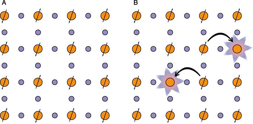
For high Tc cuprate superconductors, the most studied are those with immediately adjacent Cu-O planes. This is due to the agreed upon (by both theorists and experimentalists) notion that charge transport and superconductivity are both in the CuO2 planes. For these Cu02 planes, electron hoping from Cu to Cu is prevented due to strong Coulomb repulsion. This coupled with the fact that an anti-ferromagnetic order is energetically favorable leads to the dominating electronic state being an anti-ferromagnetic Mott Insulator (as shown in Fig 2A). In order to allow for electrons to hop between Cu and Cu, some spins must be removed from these sites (as shown in Fig 2B). Through this process, the insulating CuO2 layer becomes doped with holes or electrons, yielding new electronic ordered states; one of these states being high Tc superconductivity. As previously mentioned, the properties and characteristics of these high Tc superconductors differ from conventional superconductors. The s-wave pairing symmetry exhibited by the conventional superconductors is absent in these high Tc cuprates, for which the pairing symmetry is dx^2-y^2 symmetry. This is not the only notable difference between the two. The short coherence length, highly anisotropic critical current, and very high critical field are all different as well. One significant thing to note is that the length scales of these characteristics are all very similar in high Tc cuprates (~1 nm), while they often very by orders of magnitude in usual metals. Specifically, the Fermi wavelength is ~1 nm, the Cu-Cu distance is ~.38 nm, the inter-dopant atomic distance ~1.5 nm, and the superconducting coherence length is ~1-2 nm. Theorists and experimentalists agree that these distances suggest that different electronic phenomena can interact strongly with each other.
SI-STM
This section will discuss the use of Spectroscopic Imaging Scanning Tunneling Microscopy. This is a type of imaging technique which allows for a better look at the high Tc cuprates. Energy-resolved local DOS maps are also available for atomic resolution imaging. For this method, the conductance must be measured between the sample and the tip of the STM. This can be done using the relation g(r,V)=dI/dV. The spatial resolution will be ~1 Angstrom/pixel, with an energy resolution of ~1 meV/point. When taking into consideration that local DOS(r,E=eV) is proportional to g(r,V), the map becomes a spatial image of the local DOS at a specific energy. After this, the concept of the gap map is considered. A map with atomic resolution of the spatial dependence of the superconducting gap value delta r can be obtained. Another method which is used for the studying of Tc cuprates is the use of Fourier Transform Scanning Tunneling Spectroscopy (FT-STS). This method has been very useful in that it allows for a relation between atomic scale r-space electronic structure and k-space.
Local DOS Spectrum
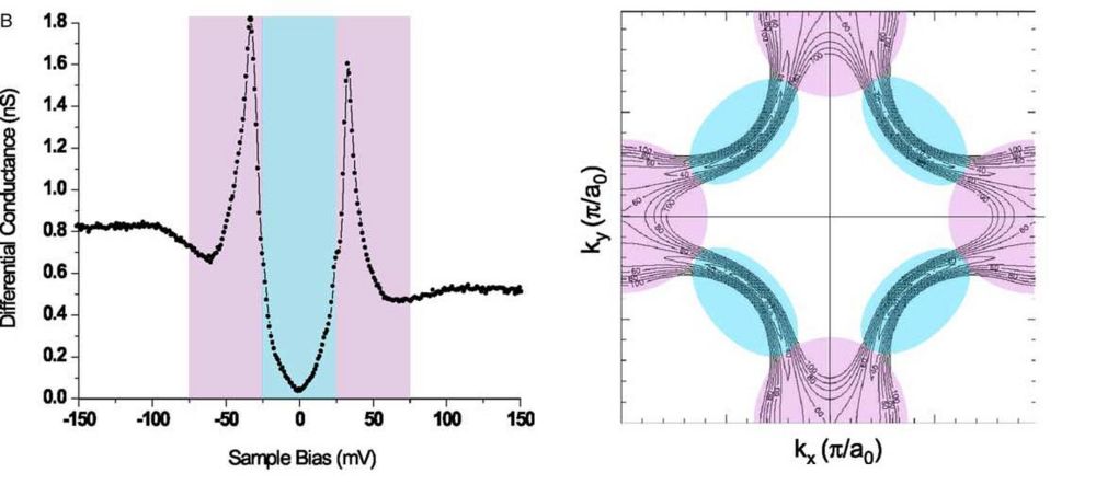 For Bi2Sr2CaCu2O(8+x), there are relatively flat BiO surfaces, with the Cu02 plane very shortly under (~5 Angstroms). This Cu02 layer is separated from the tip of the STM by thin BiO and SrO layers. Because of this, Bi2Sr2CaCu2O(8+x) is an ideal choice to better investigate high Tc cuprates. Due to this compound being a high Tc cuprate, it is believed to have a dx^2-y^2 gap symmetry. Many of the expected characteristics of the dx^2-y^2 gap structure were found in the local DOS spectrum measured of this compound (more specifically, the BiO plane of a doped sample). The above picture (left) shows a typical form for the measured LDOS at a point on this surface, with two energy regions colored differently. The picture on the right depicts a superconducting state in k-space, which allows us to view the states in space which have the same energy.
LDOS modulations
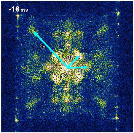
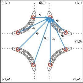
For Bi2Sr2CaCu2O8Cx, there are modulations which appear in LDOS, at energies |E|<25 meV. The use of 2D-FFT (Fig. 3) analysis was used in this case to find the wave vectors associated with the observed patterns. Analyzing the data within a scattering-induced quasiparticle interference model (shown below), the observed q vectors are in agreement with the Fermi-surface and the energy gap pictures match up with studies of dx^2-y^2 cuprate superconductors. It has been theorized that scattering most likely occurs between points of high joint DOS, which results in q-vectors which are responsible for the standing waves. Therefore, it is most likely that the modulations are from scattering centers which are related to weak scattering potentials from out-of-plane dopant atoms.
nanoscale electronic disorder
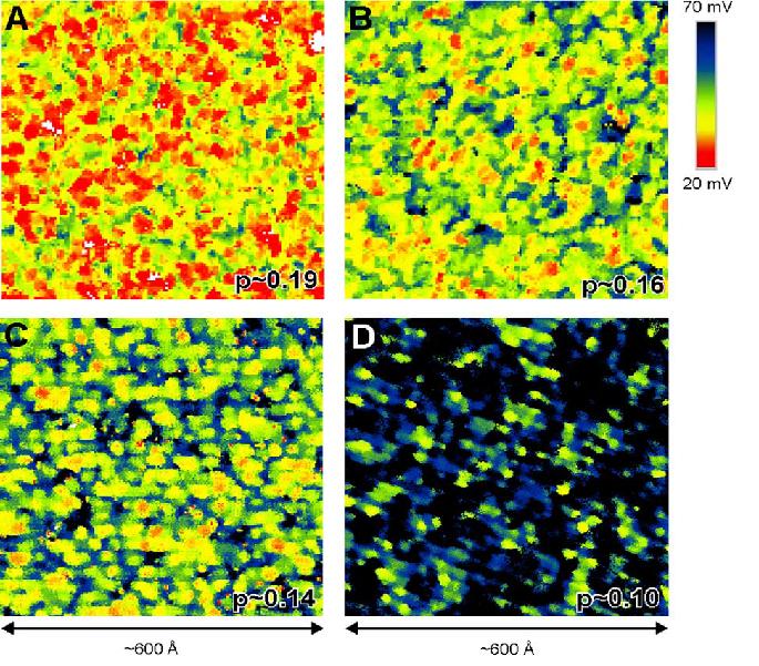
Upon looking at the doping dependence of gap maps (Fig. 4), one can see disorder of another kind. Based on the gap maps, it is evident that there is electronic disorder. It has been observed that as the doping falls, the mean gap value rises. Based on Fourier Transform Scanning Tunneling Spectroscopy (FT-STS), the same low energy quasiparticles are shared in all the regions of disorder.
This result was not something that was a focus of the study, but it has sparked some interest (as no one yet knows the source of the electronic disorder in cuprates). The research to find out more about electronic disorder and dopant atom disorder, as well as how they are related to each other, is still being carried out.
Checkerboard states
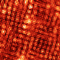
Interest in the so-called checkerboard states was started upon the use of STM on a cuprate vortex core in order to view its electron structure. These checkerboard states (as seen in Fig. 5) are a focus of much theoretical research on under-doped cuprates. In the vertex core of Bi2Sr2CaCu2O(8+x), there appears checkerboard low energy local DOS modulations. Further investigation into this led to an important discovery. It showed that, for high Tc cuprates, if one suppressed the superconductivity near the vortex core, the non-superconducting state in that high Tc cuprate can be accessed. In addition to this, it also shows checkerboard electronic crystal characteristics. Due to these discoveries, more investigation went into the relationship between checkerboard states and the high Tc superconducting phase. Another member of the high Tc cuprate family was chosen to be studied, using similar methods to those used in Bi2Sr2CaCu2O(8+x). The results from this new study agreed with those found for Bi2Sr2CaCu2O(8+x). Because of this agreement, it is believed that the checkerboard electronic crystal is related to (more specifically, a precursor to) the superconductivity and Mott insulating phase.
End Result
Through the use of Scanning Tunneling Microscopy (specifically the spectroscopic imaging Scanning Tunneling Microscopy, SI-STM), much was revealed about high Tc cuprates. The STM was necessary to understand nanoscale gap disorder, quasiparticle interference modulation and what is known as 'checkerboard' states. Along with the previously mentioned discoveries, there is new and promising evidence to suggest continued study of high Tc cuprates.
References
Hook, J.R. and H.E. Hall. Solid State Physics Second Edition. West Sussex: John Wiley & Sons, 2008.
Lee, Jinho, James A. Slezak and J.C. Davis. "Spectroscopic Imaging STM Studies of High-Tc Superconductivity." Journal of Physics and Chemistry of Solids (2005): 1370-1375.
Scanning Tunneling Microscope http://en.wikipedia.org/wiki/Scanning_tunneling_microscope
- ↑ J. Bardeen “Tunneling from a many particle point of view” Phys. Rev. Lett. 6,2 57-59 (1961)


![{\displaystyle I={\frac {4\pi e}{\hbar }}\int _{-\infty }^{+\infty }[f(E_{f}-eV)-f(E_{f}+\epsilon )]\rho _{s}(E_{f}-eV+\epsilon )\rho _{T}(E_{f}+\epsilon )|M|^{2}d\epsilon }](https://wikimedia.org/api/rest_v1/media/math/render/svg/d9e5e2cb4392f25e450d8875b6d968e44b00575e)
